How TFN signal source detects and debugs semiconductor devices and modules
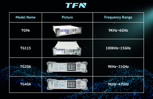
In the semiconductor industry, the performance and reliability of semiconductor devices and modules are crucial. In order to ensure that these devices and modules can meet the design requirements, TFN signal source, as a high-precision test equipment, has a wide frequency range, high signal purity, supports a variety of analog and digital modulation, provides low-frequency output and remote control interface and other functional features. It is widely used in the detection and debugging process of semiconductor devices and modules. The following will introduce in detail the process of TFN signal source detection and debugging of semiconductor devices and modules to help users better understand this process.
1. Preliminary preparation
1.1. Equipment inspection and calibration
Before any test, you first need to ensure that the TFN signal source and other related test equipment (such as oscilloscopes, vector network analyzers, etc.) are in good working condition. This includes checking whether the equipment is firmly connected, whether the power supply is stable, and whether the equipment has been recently calibrated. Calibration is an important step to ensure test accuracy and should be performed regularly.
1.2. Test environment setup
The test environment has a great impact on the test results. Therefore, it is necessary to ensure that the test environment meets relevant standards such as temperature, humidity, electromagnetic interference, etc. In addition, auxiliary equipment such as fixtures and connecting wires required for testing need to be prepared.
1.3. Test plan formulation
Develop a detailed test plan based on the characteristics and test requirements of the semiconductor devices and modules to be tested. This includes determining test parameters (such as frequency, amplitude, waveform, etc.), test steps, expected results, etc.
2. Test preparation
2.1. Connect the device under test
Properly connect the semiconductor device or module to be tested to the test system. This usually includes connecting the input of the device to the output of the TFN signal source and connecting the output of the device to the input of the oscilloscope or vector network analyzer.
2.2. Set the signal source parameters
According to the test plan, set the output parameters of the TFN signal source. This includes selecting the appropriate frequency range, setting the output amplitude, selecting the waveform type, etc. Ensure that the signal source parameters are set accurately.
3. Execute the test
3.1. Apply the signal
Start the TFN signal source and apply the preset signal to the device under test. During the test, it is necessary to pay close attention to the output state of the signal source to ensure that the signal is stable and meets the test requirements.
3.2. Collect data
Use equipment such as oscilloscopes or vector network analyzers to collect the output response data of the device under test. These data will be used for subsequent analysis and evaluation.
3.3. Repeat the test
In order to improve the accuracy and reliability of the test, it is usually necessary to repeat the test on the same device multiple times. This helps to eliminate accidental errors and improve the accuracy of the test results.
4. Data analysis and evaluation
4.1. Data processing
Process and analyze the collected data. This includes calculating statistics such as mean and standard deviation, and drawing waveform graphs, spectrum graphs and other charts.
4.2. Performance evaluation
Based on the test results, evaluate the performance of the semiconductor devices and modules under test. This includes judging whether the device meets the design requirements and whether there are performance defects.
4.3. Problem diagnosis and solution
If it is found that the test results do not meet expectations, problem diagnosis is required. By comparing the test results with the expected results, analyze the possible causes and take appropriate measures to solve them.
5. Report Generation and Summary
5.1. Report Generation
Organize the test results into a report, including test data, charts, conclusions and suggestions. The report should be clear, accurate and complete to facilitate subsequent analysis and reference.
5.2. Summary and Improvement
Summarize the test process and analyze the advantages and disadvantages of the test. Based on the summary results, propose improvement measures to improve the efficiency and accuracy of subsequent tests.
TFN signal source plays an important role in the detection and debugging process of semiconductor devices and modules. By accurately controlling the output parameters of the signal source, detailed testing and analysis of semiconductor devices and modules can be achieved. This process not only helps to ensure the quality and performance of the product, but also provides strong support for subsequent R&D and production.

If you are interested in TFN signal source, please contact TFN sales team:
Email: info@tfngj.com
WhatsApp: +86-18765219251
Facebook: https://www.facebook.com/tfnfate/
